What is photoresist etching in PCB?

Rachel Hickman
Published Feb 18, 2026
What is photoresist etching in PCB?
Photoresist Etching on PCBs Large-scale PCB manufacturers use electroplating and etching processes to produce the traces on a board. Protecting the desired copper during the etching process requires a balance between removing undesired copper and leaving the resist in place.
What are the procedures in etching the PCB?
How to Etch a PCB
- Step 1: Design.
- Step 2: Print Out the Design Onto the Shiny Side of the Transfer Paper.
- Step 3: Sand the Copper Plate So There Is a Rough Surface for the Design to Stick to When Transfered.
- Step 4: Wash the Copper With Some Water and Rubbing Alcohol and Let It Dry.
What is the solution used for etching PCB?
At one time or another, PCB manufacturing processes use solvents such as ferric chloride, cupric chloride, ammoniacal etchant, sulfuric acid + hydrogen peroxide, sulphuric and chromic acid, cupric chloride, alkaline etching, and copper ammonia complex ion as etching fluids.
What are the types of photoresist?
Types. Based on the chemical structure of photoresists, they can be classified into three types: photopolymeric, photodecomposing, photocrosslinking photoresist.
What is photoresist made of?
Photoresists are essentially hydrocarbon polymers composed of a novol-ack resin, a photoactive compound and an organic solvent. The removal of bulk photoresist patterns is typically accomplished by reaction with atomic oxygen (O), which is created in the plasma environment by dissociation of molecular O2 [221, 222].
How are etchings made?
Etching is an intaglio printmaking process in which lines or areas are incised using acid into a metal plate in order to hold the ink. In etching, the plate can be made of iron, copper, or zinc. Once the entire design has been drawn into the ground, acid is poured over the plate or the plate is dipped in acid.
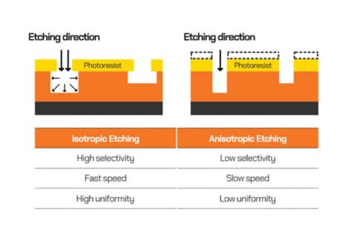
What is etching process and explain the etching methods?
Etching to create a pattern on a substrate. In semiconductor device fabrication, etching refers to any technology that will selectively remove material from a thin film on a substrate (with or without prior structures on its surface) and by this removal create a pattern of that material on the substrate.
How do you etch a PCB at home?
Dissolve 2-3 teaspoons of ferric chloride power in the water. Dip the PCB into the etching solution (Ferric chloride solution, FeCl3) for approximately 30 mins. The FeCl3 reacts with the unmasked copper and removes the unwanted copper from the PCB. This process is called Etching.
What are the two types of photoresist?
There are two types of photoresist, positive and negative resist, which are used in different applications. In positive resist, the exposed areas are solubly, in negative resist the exposed areas are insolubly for wet chemical development.
What are photoresist materials?
Photoresists are fundamental materials related to photolithography. They are light-sensitive materials, composed of a polymer, a sensitizer, and a solvent. The polymer changes its structure when it is exposed to radiation. The solvent allows the photoresist to be spun and to form thin layers over the wafer surface.
What is PCB etching and how does it work?
PCB etching is the process of removing copper from a circuit board layer that is not protected by the hardened photoresist by immersing it in a chemical solution. The etching used by industrial circuit board fabricators is broken into two different processes: acidic etching and alkaline.
What is the difference between photoresist and etch resist?
Whereas, in the inner layer, the photoresist is the etch resist. Wet etching is a type of etching process where the unwanted material is dissolved when immersed in a chemical solution. Two methods of wet etching are employed in common by the PCB manufacturers depending on the etchants used.
How do you remove the photoresist from a PCB?
Once the PCB has been exposed the transparency is removed and the plastic film which held the photoresist is peeled away. The photoresist will have hardened and will be stuck to the board. Unexposed photoresist is removed in a solution of 1% Sodium Carbonate*.
How do I remove the photoresist from the copper board?
The photoresist will have hardened and will be stuck to the board. Unexposed photoresist is removed in a solution of 1% Sodium Carbonate*. A brush is required to rapidly dissolve the unexposed areas. The copper board should be visible after this has been done.