How does a 6T SRAM cell work?

Sarah Cherry
Published Feb 25, 2026
How does a 6T SRAM cell work?
Basically, SRAM performs three operations which are Hold, Read and Write operations. Whenever the two access pass transistors of the word line (WL) are in OFF state, then the bit line and bit line bar (BL & BLB) are also in OFF condition, hence the memory cell is in hold state .
What is the difference between 6T and 8T SRAM?
8T SRAM is traditionally concerned as a more reliable memory cell, but we have managed to design 6T SRAM which executes read operation with an acceptable reliability; read being the most vulnerable operation of conventional 6T SRAM cell. Also, our 6T SRAM cell has 31% smaller area and smaller power consumption.
What are the main parts of SRAM?
Static RAM (SRAM) consists of flip-flops, a bistable circuit composed of four to six transistors. Once a flip-flop stores a bit, it keeps that value until the opposite value is stored in it. SRAM gives fast access to data, but it is physically relatively large.…
What is bit cell in SRAM?
SRAM arrays are arranged in several rows and columns of storage bit-cells called bit-lines (BL and BL’) and word-lines (WL) to control data access and storage. The bit-cells are bi-stable flip-flops which can consist of 4 to 11 transistors with pull-up (PU), pull-down (PD), and pass-gate (PG) networks.
How is a 6T SRAM cell designed to fulfill proper read and write operations?
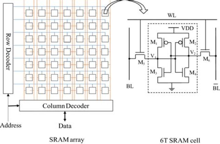
SRAM means Static Random Access Memory. The SRAM cell that we considered in this paper was 6T SRAM cell which consists of two crossly coupled inverters and access transistors to read and write the data. In case of the SRAM cell the memory built is being stored around the two cross coupled inverters.
Why is SRAM also known as 6T?
SRAM means Static Random Access Memory. The SRAM cell that we considered in this paper was 6T SRAM cell which consists of two crossly coupled inverters and access transistors to read and write the data. Therefore, SRAM is much faster when compared with the DRAM.
How many transistors are used in 6T SRAM?
Two additional access transistors serve to control the access to a storage cell during read and write operations. In addition to such six-transistor (6T) SRAM, other kinds of SRAM chips use 4, 8, 10 (4T, 8T, 10T SRAM), or more transistors per bit.
What is difference between DRAM and SRAM?
KEY DIFFERENCES: SRAM has lower access time, and is faster whereas DRAM has a higher access time and is slower compared to SRAM. SRAM users transistors and latches while DRAM uses capacitors and very few transistors. SRAM is in the form of on-chip memory, but DRAM has the characteristics of off-chip memory.
What is 6T SRAM?
How many MOSFETs are required for SRAM?
Six MOSFETs
How many MOSFETs are required for SRAM? Explanation: Six MOSFETs are required for a typical SRAM. Each bit of SRAM is stored in four transistors which form two cross-coupled inverters. 8.
What is cell ratio in 6T SRAM?
The cell ratio (CR) is the W/L ratio of the pull-down transistor to the access transistor and pull up ratio (PR) is the W/L ratio of pull-up transistor to the access transistor[4, 5]. Stability of the data stored in SRAM degrades when the supply voltage is decreased [18]. Page 6.
What is 6T static RAM?
Figure 7.18: Circuit of a 6 transistor SRAM cell. It consists of two CMOS inverters and two access MOSFETs. NBT stress mainly affects the p-channel transistors. Static random access memory (SRAM) can retain its stored information as long as power is supplied.
What is the structure of 6 transistor SRAM cell?
The structure of a 6 transistor SRAM cell, storing one bit of information, can be seen in Figure 7.18. The core of the cell is formed by two CMOS inverters, where the output potential of each inverter is fed as input into the other . This feedback loop stabilizes the inverters to their respective state.
What is the SNM of an SRAM cell?
A key figure of merit for an SRAM cell is its static noise margin (SNM). can be extracted by nesting the largest possible square in the two voltage transfer curves (VTC) of the involved CMOS inverters, as seen in Figure 7.19. The SNM is defined as the side-length of the square, given
What is meant by Random Access SRAM?
The term “random access” means that in an array of SRAM cells each cell can be read or written in any order, no matter which cell was last accessed. The structure of a 6 transistor SRAM cell, storing one bit of information, can be seen in Figure 7.18.